Timers Block - Part two
On the previous entry of this series we went through the VHDL source file and simulation of a Timer component.
In this entry, we will instantiate several Timer components to create a timer bank (or block of timers). For this purpose we will instantiate the 'Timer' component presented on the first part of the tutorial several times. The instantiation is done inside a VHDL construct called a FOR GENERATE loop (see lines 50 - 61).
The code is attached below:
1 2 3 4 5 6 7 8 9 10 11 12 13 14 15 16 17 18 19 20 21 22 23 24 25 26 27 28 29 30 31 32 33 34 35 36 37 38 39 40 41 42 43 44 45 46 47 48 49 50 51 52 53 54 55 56 57 58 59 60 61 62 | library ieee; use ieee.std_logic_1164.all; use ieee.numeric_std.all; use work.top_pack.all; entity top_timer_blk is port ( clk: in std_logic; rst: in std_logic; -- inputs data_in: in std_logic_vector (DATA_W-1 downto 0); -- Data bus, connected to all timers load: in std_logic; -- Load control common to all timers load_sel: in std_logic_vector (VEC_W-1 downto 0); -- Select what timer to load en: in std_logic_vector (TIMERS-1 downto 0); -- enable, one for each timer done_vec: out std_logic_vector (TIMERS-1 downto 0) -- done vector - one for each timer ); end top_timer_blk; architecture rtl of top_timer_blk is component timer is port ( clk: in std_logic; rst: in std_logic; -- inputs data_in: in std_logic_vector (DATA_W-1 downto 0); load: in std_logic; en: in std_logic; done: out std_logic ); end component; signal load_vec : std_logic_vector (TIMERS-1 downto 0); begin demux: process(load_sel, load) begin -- set all to 0 (default) load_vec <= (others => '0'); -- Set load signal to the addressed timer load_vec(to_integer(unsigned(load_sel))) <= load; end process; GEN_TIMER: for I in 0 to TIMERS-1 generate TMRX : timer port map ( clk => clk, rst => rst, data_in => data_in, load => load_vec(I), en => en(I), done => done_vec(I) ); end generate GEN_TIMER; end rtl; |
The load_sel signal is an address bus that selects which timer to initialize. The data used to initialize the selected timer is present at the data_in bus. When the load signal is asserted, the timer addressed by the value present on load_sel is initialized with the data on data_in.
Each timer can be enabled or disabled independently by its corresponding bit in the en vector. Any timer that reaches the timing end (value = zero), asserts its corresponding bit on the done_vec output vector. A disabled timer does not output done.
The architecture has two major blocks. The demux process delivers the load signal to the timer addressed by load_sel.
The timers themselves are instantiated on the GEN_TIMER generate loop.
The timers themselves are instantiated on the GEN_TIMER generate loop.
On the first entry of this series, the parameter DATA_W of the timer component was passed as a generic. In this article of the series we present an alternative way of parameterizing designs, namely, to use a package file. The package file for this design is shown below:
1 2 3 4 5 6 7 8 9 10 11 12 13 14 15 | library ieee; use ieee.std_logic_1164.all; use ieee.numeric_std.all; use ieee.math_real.all; package top_pack is ------------------------------------------------------------------------- -- Data size definitions ------------------------------------------------------------------------- constant DATA_W : natural := 32; -- Width of each timer constant TIMERS : natural := 16; -- Quantity of timers in block constant VEC_W : integer := integer(ceil(log2(real(TIMERS)))); end top_pack; |
As we see, the implementation consists of 16 timers of 32 bits each. Notice the usage of ceil and log2 functions to calculate the width of the addressing vector automatically from the timers' quantity.
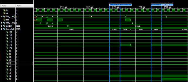
On the sample simulation, timers 0, 1 and 11 are enabled. At 490ns timer 1 reaches zero and activates its output. At 530ns timer 11 reaches its output but it is reloaded. The last two markers show when timer 11 stopped (for the second time), and last, timer 0.
As usual, the sources for the code, test bench, and waveforms, are available at Github (v1.1)
When I first did this design, we saw that the timer bank occupied significant space of a very small FPGA. So we searched for an alternative, and we used a "trick" that will be presented on the next entries of this series.
Go to the third part of this tutorial


Comments
Post a Comment